Silicon Photonics is changing the data center, with the biggest changes still ahead.

Figure 1: Google Jupiter Network for multi-thousand Ironwood TPU clusters. Source: Google
Refresher for new readers:
- Data centers contain hundreds or thousands of racks.
- For example, the Nvidia GB200 NVL72 AI compute/switch rack is about 24 inches wide, about 88 inches high and 42 inches deep. It’s called 48U because it can hold 48 1U rack servers, or 24 2U rack servers, or 16 3U rack servers.
- A rack can hold a wide range of types of servers, switches, storage and other functions.
- Scale-out in the data center refers to connections between racks, typically Ethernet.
- Scale-up refers to connections within rack, typically NVLink72/equivalent. (Scale-up will go multi-rack with optical interconnects in 3-5 years.)
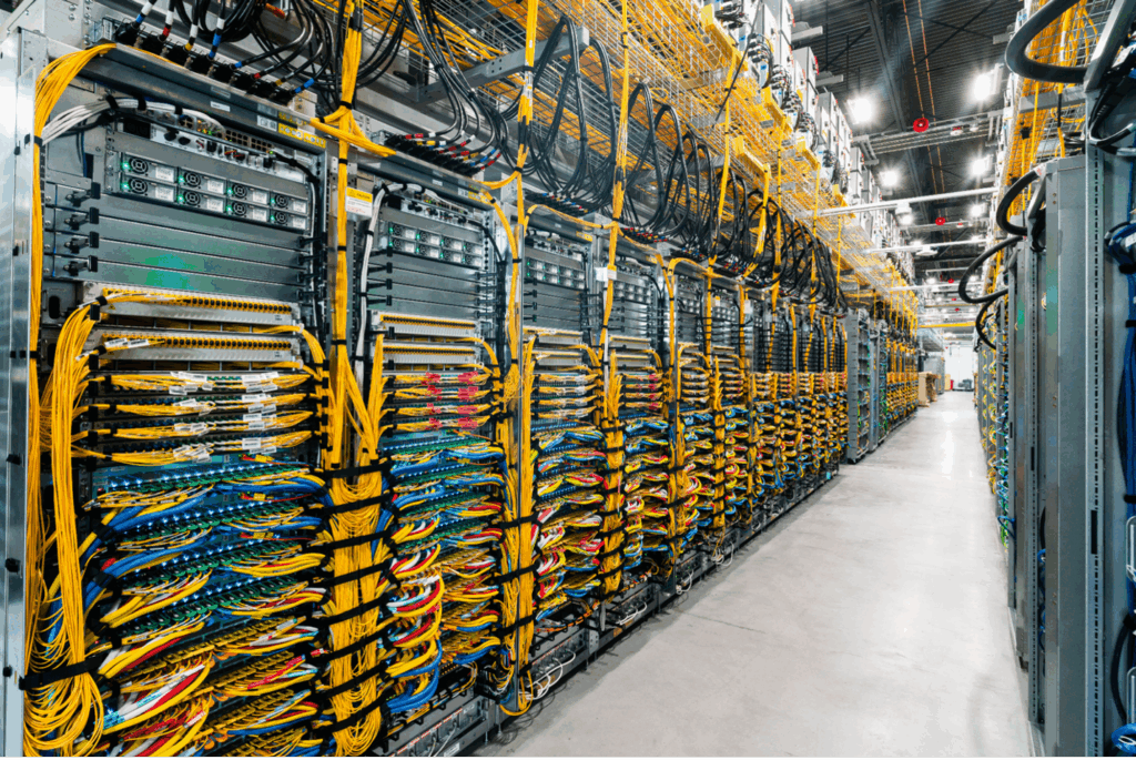
Pluggable optics have been used in the data center for some time and dominate scale-out connections. Above is a photo of Google’s Jupiter Network for interconnecting thousands of Ironwood TPUs in clusters. The bulk of the cables shown above are yellow, which signifies single-mode optical fiber (SMF). As for scale-up, Jensen Huang, Nvidia’s CEO, said last summer that “we should stay with copper for as long as we can.” Most observers think that is 2-3 more generations max.
There are a lot of connections in the scale-out network. Each rack has a top-of-rack (TOR) Ethernet switch with 128+ ports, and there are 1-2 layers of scale-out network above that. There are significantly more links in scale-up. For example, in an Nvidia NVL72 rack there are 18 switches, each of which is directly connected to every one of the 72 GPUs: 18 x 72 = 1,296 links per rack. The scale-up links per rack will grow with larger pod sizes NVL144 then NVL576. So when scale-up goes optical, the optical market will grow much larger.
At OFC 2025, an OMDIA forecast of the total optical components showed the total market had grown from a few billion $ in 2003 (mostly telecom) to about $13 billion in 2023, at which point growth sharply accelerates with forecasts of $25 billion by 2030, primarily due to the growth in AI networking. First, scale-out. And in a few years, scale-up. A more recent CignalAI forecast predicts the total market to be $31 billion in 2029.

Figure 2: Total optical components market. Sources: OMDIA & CignalAI
Optical components consist of:
- Silicon photonics, which integrates photonic devices that used to be discrete onto a modified CMOS process;
- Lasers, silicon optical amplifiers (SOAs), and other devices that are built on III-V processes like InP (Indium Phosphide) and GaAs (Gallium Arsenide), and
- Packaging, fibers, connectors, adapters that provide the connections between the chips.
This article focuses on silicon photonics. A future article will discuss the other key components.
How light transfers data between chips
Copper in the data center is transitioning to optical. The actual physical optical connections are made by fiber optics cables that typically are “single-mode fiber,” which carry light of a single mode and single or multiple wavelengths. The layers of cladding protect the fiber, but more importantly, they have lower refractive indexes than the core so light remains concentrated in the fiber. Fiber optic cable is a big business. Corning, a market leader, sells $6.8 billion/year worth of fiber optics. Meta just did a $6 billion deal with Corning for fiber-optic cable over several years.

Figure 3: A Single-Mode Fiber cable – the actual fiber is 8-9mm diameter of a 2-3mm cable (source: Wikipedia, Creative Commons License: CC BY-SA 3.0)
The actual optical fiber, made of glass, is extremely thin — 9mm, or 1/100th of a millimeter. The very narrow diameter keeps light in single-mode, which is what silicon photonics uses.
The wavelengths are used in fiber optics are O-band, E-band, S-band, C-band and L-band, because they have relatively low signal loss in optical fibers. These are all in the infrared spectrum.

Figure 4: Optical transmission bands in fiber optics. Source: Claude.ai
The O-band is used in silicon photonics because of its low transmission loss in silicon waveguides.
In a fiber, or on a chip’s wave guide, there can be single or multiple wavelengths used. Multiple wavelengths can be accommodated in two ways: CWDM or DWDM. CWDM is Coarse Wave Division Multiplexing, in which the wavelengths are spaced relatively far apart. DWDM is Dense Wave Division Multiplexing, in which the wavelengths are spaced relatively close together. CWDM and DWDM both deliver more bandwidth, but they have different implementation challenges.
Note that even though almost all optical fibers used for interconnect are SMF (single mode fiber) they are not necessarily interoperable because the light can be transmitted on single or multiple wavelengths, different wavelengths, and/or use different connectors.
Silicon Photonics Applications
Pluggable Optics
The data center main market driver today for silicon photonics is pluggable optics transceivers.
They are a standardized, hot-pluggable device connecting to the electrical interface of a switch or server on one side, and to fiber optics on the other. They enable the high-speed transmission of data from one switch/server to another over fiber optics at much higher bandwidth and at much lower power than the copper cables they have replaced.
The major components of the pluggable optics transceiver are 1) a laser, 2) a CMOS chip with DSP functionality and a high-speed SerDes, and 3) a silicon photonics chip. The silicon photonics modulator, typically Mach Zehnder in these transceivers, modulates the laser light to superimpose the data from the CMOS electrical chip. There are also filters, couplers, garnets, lenses, and isolators. This is all packaged in a standardized pluggable format.
Coherent’s 2025 Investor Presentation projects the market for pluggable optics as growing from $6 Billion in 2023 to $25 Billion in 2030! By 2030, the market will be primarily 1.6T (1.6 terabits/second) and 3.2T data rates, with some slower legacy products still shipping.
Optical Circuit Switches (OCS)
Google has used Optical Circuit Switches (OCS) in Google Cloud for years.
Unlike other AI accelerators, Google’s TPUs are switchless, using a three-dimensional routing structure that enables pods of thousands of TPUs. Their TOR (top-of-rack) switches use pluggable optics and are connected to an OCS layer that enables reconfiguration of top-level interconnects across the whole data center. This proves very valuable for redundancy, reliability and network reconfiguration for changing workloads. Google’s approach uses MEMs (Micro-Electro-Mechanical) mirrors, which are arranged to take hundreds of incoming fibers and steer the light paths to any of hundreds of outgoing fibers.

Figure 5: Google OCS uses MEMs Mirrors to route/switch light. Source: Google.com
Lumentum and Coherent are now also offering OCS, using MEMS (Lumentum) or liquid crystal (Coherent). At a financial conference in December 2025, Coherent’s CEO said, “We love OCS.” Last summer, they projected the TAM to be over $2 billion, but now see larger customer interest and more applications, so they’ve upped their TAM estimate to over $3 billion.
Several startups are developing “two-dimensional” OCS using more compact silicon photonics approaches. These include iPronics, nEye and Salience. All are sampling proof of concept (nEye, Salience) or shipping initial product (iPronics). These could eventually be cheaper or more reliable than existing architectures. These higher density solutions also might enable OCS to penetrate scale-up connections, first for redundancy/reliability, and later for all-GPU-to-all-GPU OCS connections, perhaps even one day eliminating silicon packet switches for scale-up.
Co-Packaged Optics (CPO)
CPO enables higher density and lower power than pluggable optics.
CPO has begun to encroach on pluggable with the announcements by Nvidia and Broadcom in 2025 of ethernet scale-out switches using co-packaged optics to cut the power of switching.

Figure 6: Nvidia Spectrum-X scale-out switch with CPO, Nvidia GTC 2025. Source: iPronics
The switches are the two chips (in the red box above) topped by a liquid cooling enclosure. The four thick black cables coming from the top are liquid-in, liquid-out. The pluggable lasers (in the green box above) that provide the carrier wave for signaling are on the top of the box at the bottom of the picture. There are 9 of them, with probably 8 lasers in each. You can see 9 yellow cables going from the lasers to the switch chips. Lasers are pluggable because they have a higher failure rate, so they can be replaced easily when they fail without requiring the whole switch be changed. Only one input fiber is connected at the bottom left corner – the yellow cable. You can see there are numerous additional fiber connectors. The fiber connections from the I/O panel to the chips must be routed underneath what we can see.
The power savings of CPO (1/3 of the power of pluggable) are extremely significant for scale-up because there are 1,000+ connections per rack. Nvidia, Broadcom, Ayar Labs, Celestial (recently acquired by Marvell), Lightmatter and Ranovus all are working on CPO solutions.

Figure 7: What an AI accelerator with CPO will look like. Source: Ayar Labs
Today, all GPU/XPU/AI accelerators use copper connections. As Nvidia’s Huang noted, the push is to use copper for as long as possible. But copper is nearing a wall of diminishing returns, where higher performance leads to too-short connections and higher error rates. Optical connections will enable AI accelerators to continue to grow the interconnection bandwidths at low latencies and much larger pod sizes.
Ayar Labs, with Alchip, showed late last year a concept of what an AI accelerator will look like with CPO. The accelerator and HBM chiplets are on the silicon interposer, and the optical engine chiplets (8 shown here, with over 256 fibers) are mounted on the organic substrate. At some point, the optical engines will go directly on the interposer.
Silicon photonics foundries will see huge growth; TSMC may become #1
Compared to CMOS, silicon photonics manufacturing today is small-scale.
The major silicon photonics foundry players today are GlobalFoundries (which recently acquired AMF) and Tower Semiconductor. There are smaller players as well, such as imec for prototyping, LioniX in the Netherlands, and Silterra in Malaysia. In the Chinese market, SMIC offers silicon photonics. TSMC, Samsung, and UMC are all developing silicon photonics capabilities for their foundry offerings.
GlobalFoundries (GF), with its acquisition of AMF, claims to be the #1 silicon photonics (SiPho) foundry, with almost $300M SiPho revenue expected in 2026 and >$1 billion expected by the end of the decade. Kevin Soukup, VP/GM of silicon photonics at GF, explained to me that in Singapore, they now have two fabs focused on C Band and L Band, primarily for long-haul coherent applications. One is the AMF fab they acquired, in addition to their original, much larger fab that runs the AMF process, as well. Using their larger fab, they can greatly grow capacity for their long-haul customers. In Malta, their SiPho fab focuses on pluggable transceivers and co-packaged optics. They have a process that fabricates 45nm CMOS on chip with RF and/or silicon photonics. They can also do SiPho chips with no CMOS. They use advanced equipment from their 12nm finFet process to build lower-loss waveguides. They also have a process similar to TSMC’s COUPE, which combines an electrical interface chip (EIC) with a photonics integrated chip (PIC) into a single chiplet. They support edge connection and top connection for fiber inputs, but unlike COUPE, they use an optical mirror for the top connection to reflect the light 90 degrees to an edge connection, which eliminates the need for a grating coupler. This gives them an advantage in broadband, because grating couplers have difficulty handling broadband. Soukup said they have customers “designed-in” using GF’s CPO capability for scale-out and scale-up.
GF also projects 2026 revenues for the #2 SiPho foundry at ~$200M, #3 at ~$100M, #4 at ~$50M. Adding this up and estimating the rest of the foundries, 2026 SiPho foundry revenues will be less than $1 B/year. This is less than 1{2d86e206823e03865fa8be0e21e9a6ee7441ee8bfd1fad108302568e2129cc3f} of TSMC’s annual revenues.
Tower Semi appears to be the second largest silicon photonics foundry.
Some companies make their own silicon photonics, such as Intel, and ST Micro. Many other semiconductor/systems companies sell silicon photonics products that are manufactured at a foundry – for example, Cisco uses GlobalFoundries.

Figure 8: Silicon photonics wafer revenue forecast. Source: GlobalFoundries
Data center AI is driving a dramatic ramp in the growth of silicon photonics foundries: 8X growth in just 6 years, from 2026 to 2032. Scale-out is the major driver now. Scale-up will become the biggest driver in a few years, as there are far more links in scale-up in a data center.
The market value of the silicon photonics chips when sold will be much larger because the packaging can cost as much as the chip, and margins are >50{2d86e206823e03865fa8be0e21e9a6ee7441ee8bfd1fad108302568e2129cc3f}. DataM Intelligence projects the silicon photonics IC market will reach $32B by 2031; Precedence Research projects $29B by 2034.
Scale-out has begun moving to CPO, and scale-up will need CPO in the near future. Scale-up needs CPO because the PICs (photonic integrated circuits) must be small enough to fit many of them on the edge of a GPU with numerous fiber connections per PIC. This requires miniaturization of key circuitry in the PIC, especially the Modulator which is typically Micro-Ring instead of the much larger Mach-Zehnder modulator used in pluggable optics. Scale-out is moving to CPO because power dissipation is 2/3 less than for pluggable optics: every watt saved in networking is a watt that can be used for compute which makes the money.
TSMC currently makes essentially all AI Accelerator chips for Nvidia, AMD, Google, AWS, and others. These chips consist of numerous chiplets (GPU/XPU, HBM, I/O). TSMC requires that all chiplets in the package are made by TSMC, following their PDK (process development kit) and specs, to ensure proper operation and high yield. This means all silicon photonics chiplets that TSMC integrates will be made by TSMC. For some time, TSMC has been developing its COUPE process (IEEE ECTC 2025 paper, “Optical and Electrical Characterization of a Compact Universal Photonic Engine”). Most likely, they have been developing this in response to requests from their biggest customers, Nvidia and Broadcom, both of which have begun deploying COUPE in their scale-out switches in the last year.
Given that a) 8X growth in SiPho Foundry revenues will require major CapEx, and b) TSMC currently builds all the non-HBM chiplets in AI accelerators, it seems likely that in the next five years TSMC will move from zero in silicon photonics to the #1 SiPho foundry as AI accelerators transition to CPO. There is some CoWoS capacity at ASE, etc., so there could be some non-TSMC CPO on organic substrates. Or, GF or its major customers could convince TSMC to use GF-manufactured Optical Engine chiplets – GF is not a competitive threat to TSMC for AI accelerators since its most advanced node is 12nm.
Silicon photonics devices, designs, and chips
A CMOS designer is used to a 1,000 page PDK with extensive rules and formulas. These include multiple libraries of devices supplied by the foundry, which will work together if you follow the rules, and numerous large, complex IPs of entire subsystems.
Silicon photonics today is like silicon design in the 1980s, when a fab had limited documentation, a ring oscillator to show performance, and the designer had to build their own device libraries and model everything from SPICE up. The growth of silicon photonics, and the entry of TSMC into silicon photonics, will likely bring much more structure and foundational IP in the next five years. Companies like Synopsys and Cadence do offer silicon photonics design tools, but many of the structures designers are developing are new and require very detailed, time-consuming, low-level modeling from the fundamental physics.

Figure 9: Typical library components of a photonic IC platform: generation, routing, processing, detection and modulation. Source: Review of Silicon Photonics Technology and Platform Development, SY Siew et al, 2021, Journal of Lightwave Technology under Creative Commons Attribution 4.0 license
Silicon photonics is manufactured on 200mm and 300mm wafers, down to 65nm. The wafer used is SOI with a thick buried oxide layer (BOX: SiO2) at least 1 micron thick for optical isolation. The reason for this, as shown below, is that single-mode light transmitting in a silicon (or silicon nitride) waveguide propagates primarily within the silicon waveguide core, but some of the light field “leaks” into the adjacent materials on top, on the side, and below. So these layers need to thick enough that the light doesn’t propagate into other active areas.

Figure 10: Single-mode light in a wave guide “leaks” into surrounding material. Source: Claude.ai
A big challenge in silicon photonics is signal loss — the strength of signal at the input of a waveguide faces losses for each unit of distance traversed in the waveguide. All of the devices that manipulate light have signal losses, as well. If the signal loss accumulation is too high, the signals are no longer strong enough for operation. So careful attention to the signal loss budget is critical in silicon photonics design.
In silicon photonics, there generally are no CMOS transistors (the integration of SiPho and CMOS has begun – GF has a process that combines the two – but it is not yet common). The devices available in a silicon photonics process typically are:
- Routing: Waveguides, made of silicon and silicon nitride. The waveguides need a certain height and width for light to be single-mode, and the waveguides need to be surrounded by sufficient material so light doesn’t interact with other elements. Waveguides can’t turn corners at a sharp 90 degrees. The bend needs a minimum radius so light is refracted within the waveguide. Interestingly, two waveguides can cross at right angles with minimal interaction between the perpendicular beams. This is important because many foundries only have one layer of waveguide.
- Detection: This comes in two categories, couplers and photodetectors. Couplers are used to capture light coming onto the chip from a fiber. The most efficient way to couple light into the chip is with edge couplers, but alignment of the fiber and the chip can be challenging. The easiest way to align the fiber for coupling with the chip is from above to a grating coupler. A 1D (1-dimensional) grating coupler is used for polarized light, a 2D grating coupler is for unpolarized light. Polarized fibers are much, much more expensive than standard SMF, so they are typically only used from the laser to the chip – so lasers are brought on chip with 1D grating couplers, which have lower signal loss. 2D grating couplers can capture unpolarized light, but are bigger, more complicated, and have larger signal loss. They’re used for data signals. Photodetectors are used to convert the intensity of light in a waveguide into an electrical signal that can be read by a companion CMOS chip. Photodetectors are made using germanium, which is not a normal material in a CMOS fab.
- Modulation: Modulators are used to transfer electrical signals onto a light signal. In pluggable optics, the modulator is Mach-Zehnder. In CPO, the modulator is a micro-ring, which is a much smaller device, critical for making the CPO chiplet small enough to bring in dozens of fibers into a small space to couple to the GPU. Heaters, shown in the diagram below, are used to control modulators to insert bits into an incoming laser stream based on the electrical signals from a companion CMOS chip. At high speeds, this requires high-speed PHYs to drive the modulator controls. Mechanical stress and voltage can also be used as controls for photonic devices.
- Processing: Mach-Zender devices in an interferometer configuration can be used to create an optical switch that takes two incoming light streams and drive them out to two outgoing light streams. By controlling heaters, the switch can either be configured to take input 0 to output 0 and input 1 to output 1, or it can be configured to take input 0 to output 1 and input 1 to output 0. These switches can switch as fast as microseconds.

Figure 11: Cross sectional view of AMF’s (now GF) standard MPW (Multi Project Wafer) Flow. Source: Review of Silicon Photonics Technology and Platform Development, SY Siew et al, 2021, Journal of Lightwave Technology under Creative Commons Attribution 4.0 license
The oxide window shown above is used for photonic sensors of bio/chemical so they can interact with the light field. This is not an application used in the data center.
Typically, silicon photonics chips do not have CMOS devices. Photonics devices are physically large compared to CMOS transistors. For example, has CMOS and SiPho at 45nm. Although some photonics device features would benefit from advanced lithography, photonics will not be integrated into 3nm or 2nm any time soon, if ever.

Figure 12: A silicon photonics chip, schematic and die photo. Source: Quack et al., Microsystems & Nanoengineering, 2023 – Creative Commons Attribution 4.0 International License
Silicon photonics will be everywhere in the 2030 data center
Using silicon photonics, chips doing complex manipulation of light are now possible. As shown above, the structures are physically large, like in early CMOS. The primary function of silicon photonics in the data center is data transmission between very high-performance CMOS compute chips and switches, and probably memory pools. These silicon photonics chips will increasingly be found integrated into every unit in the data center, and we will get very used to seeing boards with bright yellow fibers carrying high-bandwidth data. Server microprocessors will probably be next, replacing PCIe (Peripheral Component Interconnect) with optics.
The industry structure of silicon photonics manufacturing will be similarly revolutionized with an order of magnitude growth in wafer revenues, and the rise of TSMC as likely the largest supplier due to their role in making all the chiplets, including the optical engine, in AI accelerators. TSMC is likely to bring a lot of the structure and infrastructure to SiPho as they have with CMOS, which will enable the development of more complex photonics chips in less time and at lower cost.